Smartphones, Digital Cameras, Autos and Medicine Drive Image Sensor Demand
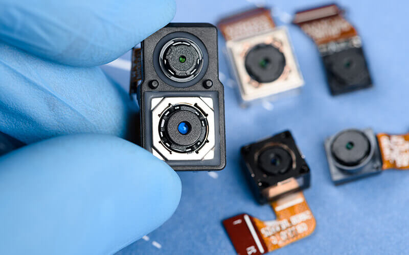
An image sensor is a semiconductor that captures digital images and videos, and its performance can be determined through image quality, speed and power consumption. Demand for these sensors is growing rapidly because of their imaging capabilities in smartphones, digital cameras, automobiles and medical devices. What is more, image sensors are being combined with advanced AI algorithms to enable object recognition, scene analysis and real-time decision-making.
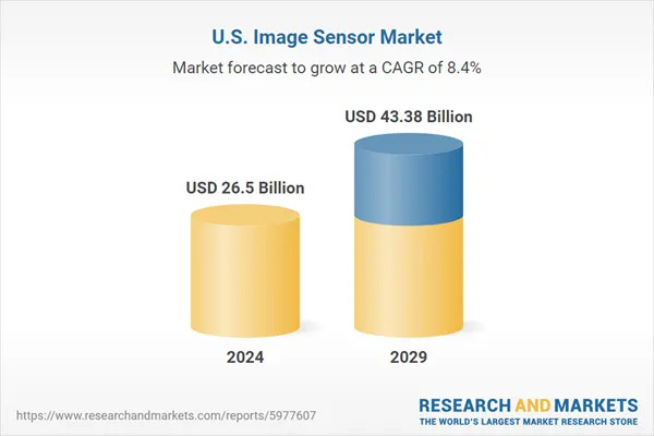
According to ResearchAndMarkets.com's study “The United States Image Sensor Market, Competition, Forecast and Opportunities, 2019-2029,” the market was valued at $26.5 billion in 2023 and is anticipated to achieve robust growth in the forecast period with a CAGR of 8.4% through 2029. This potential has attracted numerous competitors. Let’s take a look at some of the new and notable products and technologies recently offered.
Samsung Electronics has announced three new mobile image sensors designed for both main and sub cameras in smartphones: the ISOCELL HP9, the ISOCELL GNJ and the ISOCELL JN5.
The ISOCELL HP9 features 200 million 0.56-micrometer (μm) pixels in a 1/1.4-inch optical format. With its proprietary high-refractive microlens including a new (but unnamed) material, the HP9 enhances light-gathering capability by directing more light accurately to the corresponding RGB color filter. This results in improved color reproduction and focus with 12% better light sensitivity (based on signal-to-noise ratio 10) and 10% improved autofocus contrast performance compared to the previous product, according to Samsung.
As main cameras in premium smartphones grow in size, room for telephoto cameras is also increasing. The HP9’s large optical format makes it suitable for telephoto modules, delivering performance that is said to match premium main cameras in image quality, autofocus, high dynamic range (HDR) and frames per second (fps).
Powered by a remosaic algorithm – an interpolation procedure that rearranges pixels to improve image resolution and quality in different lighting conditions – the HP9 offers 2x or 4x in-sensor zoom modes, achieving up to 12x zoom when paired with a 3x zoom telephoto module.
The Samsung ISOCELL GNJ is a dual pixel sensor with 50 million 1.0μm pixels in a 1/1.57-inch optical format. Each pixel houses two photodiodes, enabling fast and accurate autofocus, similar to the way human eyes focus. The image sensor also simultaneously captures full color information for quick focusing with sustained image quality.
The newly improved high-transmittance anti-refractive layer (ARL), coupled with Samsung’s proprietary high-refractive microlens is said to boost light transmission and reduce unwanted reflections but also ensuring that dark areas are not overly brightened for more accurate photos with well-preserved image details. These innovations have been achieved with less power consumption, featuring a 29% improvement in preview mode and 34% in video mode at 4K 60fps, according to the company.
The ISOCELL JN5 features 50 million 0.64μm pixels in a 1/2.76-inch optical format. Dual vertical transfer gate technology increases charge transfer within pixels, substantially reducing noise in extreme low light conditions for clearer image quality.
Leveraging Super Quad Phase Detection (Super QPD), the JN5 adjusts focus by comparing phase differences both vertically and horizontally, catching small details of rapidly moving objects with minimal shake.
Additionally, the JN5 incorporates dual slope gain (DSG) technology to enhance its HDR. This technology amplifies the analog light information entering the pixels into two signals, converts them into digital and then combines them into one data set, expanding the range of colors that the sensor can produce.
The JN5’s slim optical format allows it to be used across main and sub cameras — including wide-angle, ultra-wide-angle, front and telephoto units.
STMicroelectronics has introduced a set of plug-and-play hardware kits, evaluation camera modules and software that ease development with its ST BrightSense global-shutter image sensors. By sampling all pixels simultaneously, unlike a conventional rolling shutter, global-shutter sensors can capture images of fast-moving objects without distortion and significantly reduce power when coupled to a lighting system.
ST BrightSense CMOS global-shutter sensors implement backside-illuminated pixel technology, manufactured at ST’s own foundry in France, ensuring high image sharpness to capture fine details such as in barcode reading. Their high sensitivity enhances low-light performance and permits fast image capture, enhancing responses such as obstacle avoidance in mobile robots and face recognition in personal electronics. The sensor’s advanced 3D-stacked construction allows a small die area, easing integration anywhere space is limited especially in the final optical module while providing on-chip image processing for auto-exposure, correction and calibration. An MIPI-CSI-2 interface makes them well-suited for embedded vision and edge AI devices.
ST’s new offering includes evaluation camera modules that integrate image sensor, lens holder, lens, and plug-and-play flex connector to facilitate integration of the image sensors. The modules offer a selection of tiny form factors down to 5mm2, various lens options to suit different application requirements and a plug-and-play connector that allows easy swapping. A series of hardware kits helps developers integrate the sensors with various desktop and embedded computing platforms.
Complementary software tools are available for free download on ST’s website, such as a PC-based GUI and Linux drivers that assist integration with popular processing platforms including STM32MP2 microprocessors.
The ST BrightSense global-shutter family currently comprises the VD55G0, VD55G1 and VD56G3 monochrome sensors with resolution from 0.38Mpixel to 1.5Mpixel, as well as the color VD66GY with 1.5Mpixel. The sensors, along with their evaluation camera modules, and development boards are in production now.
OMNIVISION has announced the new OG0TC BSI global shutter image sensor for eye and face tracking in AR/VR/MR consumer headsets and glasses. With a package size of just 1.64mm x 1.64mm, the OG0TC is aimed primarily at inward-facing tracking cameras. This small form factor is key to industrial designs as multiple cameras are required for tracking all aspects of the face (eyes, brows, lips, etc.). The OG0TC is pin-to-pin compatible with OMNIVISION’s previous-generation BSI GS image sensor.
The OG0TC BSI GS image sensor is said by the company to reduce power by more than 40% (at 30 frames per second) over its previous-generation OG0TB sensor.
The sensor is built on OMNIVISION’s PureCel Plus-S stacked-die technology. In low-light conditions, PureCel Plus pixel technology picks up more light than previous generations by significantly enhancing sensor sensitivity and capacity, which boosts low-light performance with lower SNR10 (a metric for measuring a color image sensor's noise properties with one single number) and higher dynamic range. Reducing color crosstalk further improves color reproduction.
The OG0TC GS image sensor is available now for sampling and is in mass production.
Teledyne DALSA’s AxCIS family of high-speed, high-resolution integrated line scan imaging modules is now available in color. These contact image sensors (CIS) combine sensors, lenses and lights offering a lower cost inspection system for machine vision applications including battery and print inspection.
Powered by Teledyne’s CMOS image sensors, AxCIS delivers up to a 60 kHz x 3-line rate of native RGB colors at a pixel size of 28 µm or 900 dpi resolution so defects can be detected with precision. Its sensor design is said to cover the entire field of view without missing pixels, providing a 100% seamless image without interpolation. In addition to defect detection, its design also supports true metrology applications.
AxCIS has a single 24V power supply and can fit in a system even with limited vertical clearance. Its Camera Link HS SFP+ fiber optic interface delivers high throughput data over standard long-length cables with immunity to EMI radiation for harsh industrial environments.
Follow TTI, Inc. on LinkedIn for more news and market insights.
Statements of fact and opinions expressed in posts by contributors are the responsibility of the authors alone and do not imply an opinion of the officers or the representatives of TTI, Inc. or the TTI Family of Specialists.
Follow TTI, Inc. - Europe on LinkedIn for more news and market insights.
Statements of fact and opinions expressed in posts by contributors are the responsibility of the authors alone and do not imply an opinion of the officers or the representatives of TTI, Inc. or the TTI Family of Specialists.